Started construction in Taiwan’s Silicon Valley
TSMC’s largest business… mass production in 2025
Competition heats up for foundry leadership
Taiwan’s TSMC, the world’s largest semiconductor consignment manufacturing (foundry) company, has begun construction of a new plant to produce semiconductors based on the ‘2nm (nanometer · 1nm = 1 billionth of a meter)’ process in Hsinchu, called ‘Taiwan’s Silicon Valley’. Japan’s Nihon Keizai Shimbun (Nikkei) reported on the 23rd.
TSMC started mass production of ‘3nm’ semiconductors at the end of last year. It immediately prepared for mass production of ‘2-nano’ semiconductors without any time to breathe, revealing its determination not to lose its position as the No. 1 company to competitors such as Samsung Electronics in Korea.
Samsung succeeded in mass-producing 3-nano semiconductors for the first time in the world ahead of TSMC in June of last year. Samsung is also speeding up construction of foundry plants in Taylor, Texas, USA, and Pyeongtaek, Gyeonggi, with the goal of operating them in the second half of next year. In a situation where the economy of the semiconductor industry is not the same as before due to the global economic slowdown and the strengthening of US regulations on semiconductors in China, major companies are competing with astronomical amounts of money, drawing great attention.

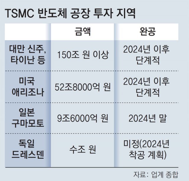
Hsinchu is about 60 km southwest of Taipei, the capital of Taiwan. TSMC headquarters and numerous semiconductor companies are concentrated here. TSMC is building a new 2nm plant by securing land 2.5 times the size of the Seoul World Cup Stadium in Mapo-gu, Seoul. According to Nikkei, at least 2 trillion yen (about 20 trillion won) is needed to build just one 2-nano plant. TSMC decided to build four such factories. This means at least 80 trillion won will be invested. This is the largest project in TSMC’s history, and mass production will begin in 2025 at the earliest. Previously, Samsung announced plans to mass-produce 2-nano semiconductors in 2025 and 1.4-nano processes in 2027. Foundries have higher added value and less inventory risk than memory semiconductors such as DRAM, which are mainly produced by domestic companies such as Samsung and SK Hynix. In addition to large-scale production facilities, it requires top-notch manufacturing technology and patents, so entry barriers are significant.
Samsung has been investing heavily in the foundry field for years, but it is showing a significant gap with TSMC. According to Taiwanese market research firm ‘TrendForce’, TSMC’s global market share as of the fourth quarter of last year (October-December) was 58.5%, more than three times that of Samsung (15.8%). An official from the Japanese semiconductor industry also told Nikkei, “Samsung is struggling because its yield has not risen. US Intel fell further behind, and the era of’TSMC’s 1st round’ has arrived in the 2020s.”
Although TSMC’s market share is significantly ahead, the competition between Samsung and TSMC over supremacy in the foundry market is intensifying. These two companies are the only companies in the world that are mass-producing 5-nano foundries.
Samsung is targeting the start of operation of its plant in Texas in the second half of next year (July to December). The third plant in Pyeongtaek also aims to start operation in the second half of next year. Earlier on the 15th, it claimed to be a ‘system semiconductor mecca’ and said, “We will invest more than 300 trillion won in the Yongin cluster in Gyeonggi-do over the next 20 years to create a high-tech memory and foundry production base.”
In order for Samsung to catch up with TSMC, which is the firm leader, it is essential to expand production capacity in the mid- to long-term. Accordingly, it plans to maintain its annual investment in the semiconductor sector of around 50 trillion won despite the cold wave of the semiconductor economy and the recent slowdown in performance.
Jeong Ki-bong, Vice President of Foundry Business Department at Samsung Electronics, emphasized that he would secure a foothold for future growth engines by strengthening technological competitiveness, saying, “We will expand new orders from 3-nano 2nd-generation customers and focus on developing 2-nano 1st-generation semiconductors.”
Tokyo =
Source: Donga
Mark Jones is a world traveler and journalist for News Rebeat. With a curious mind and a love of adventure, Mark brings a unique perspective to the latest global events and provides in-depth and thought-provoking coverage of the world at large.